WE DETERMINE THE STRUCTURE OF THE PRODUCT
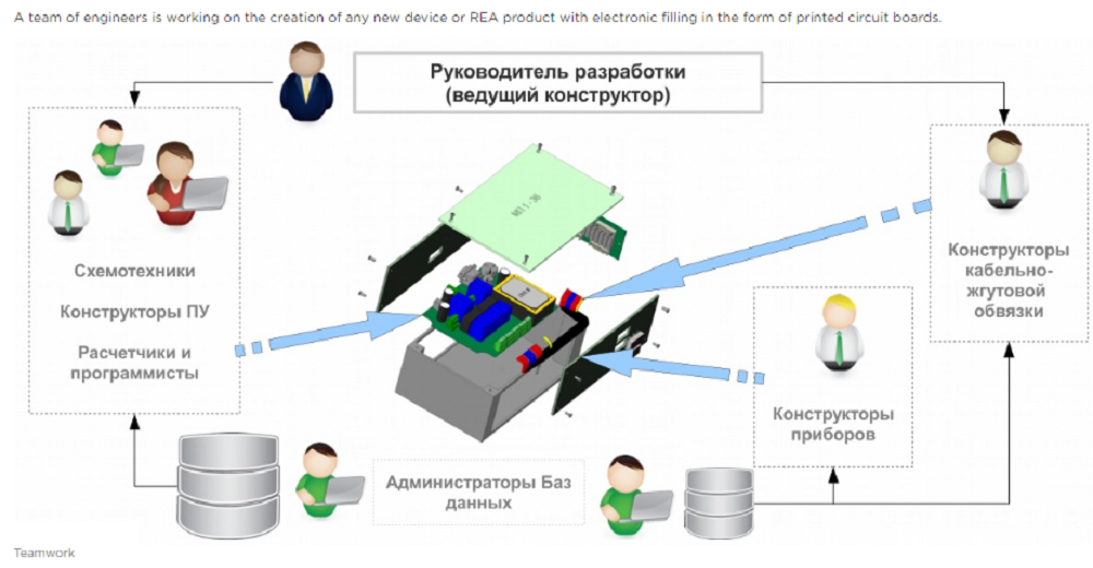
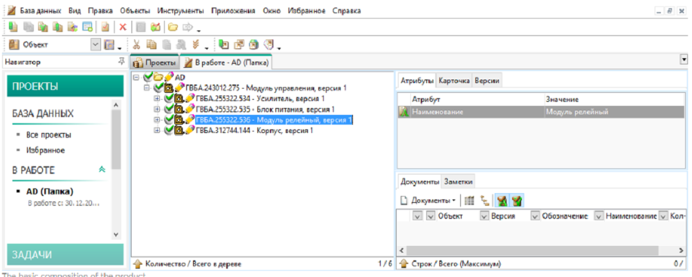
The process of design engineering begins with the determination of the basic structure of the future product - the division scheme. The skeleton, on which specific components and various types of documents and data will be further built up, can be considered the basic set of assembly units registered by the leading designer in the environment of the LOTSMAN: PLM product data management system.
WE DESIGN AN ELECTRONIC “STUFFING” IN A MECHANICAL “ENVIRONMENT”
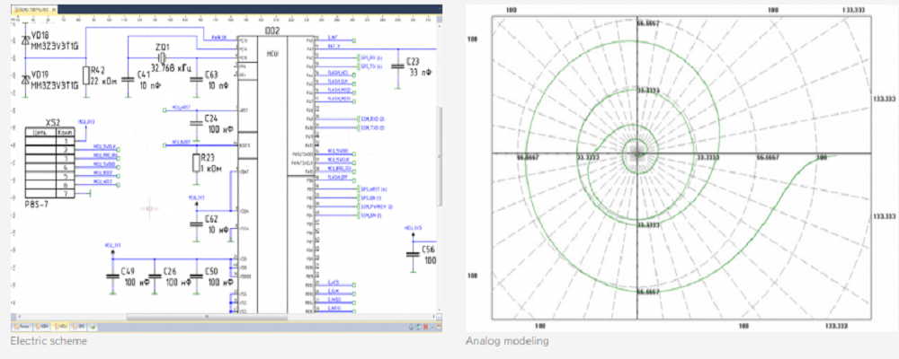
The lead designer formulates the problem for circuit designers who develop electrical circuit diagrams into separate modules in the printed circuit board design system (ECAD system) using a database of electronic radio products and components (ERI) and simulate the operation of the circuit. An example of an ECAD system is the Russian Delta Design product of Eremex.
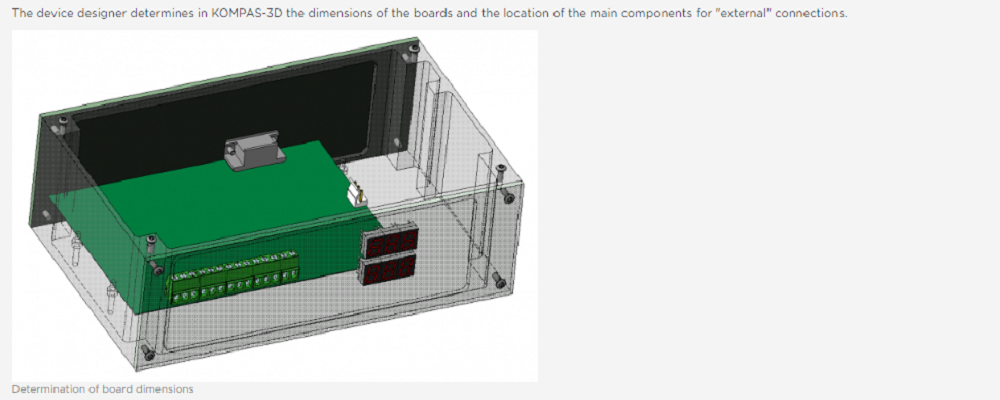
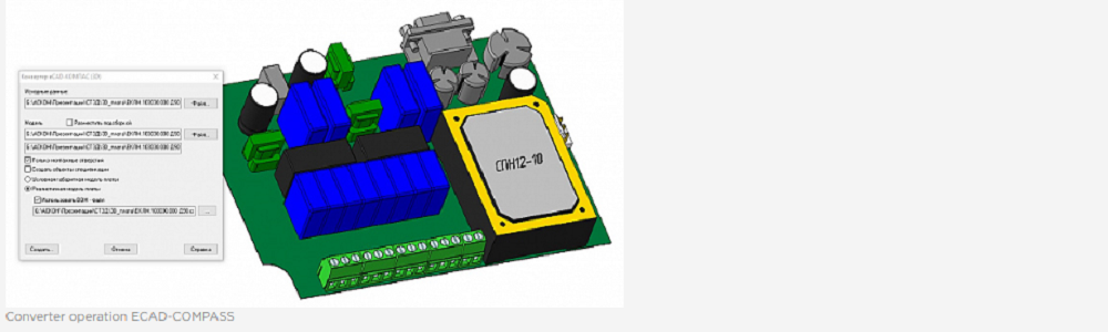
Now it is important to transfer this data to the ECAD system. For this, KOMPAS-3D has a special KOMPAS-IDF Converter module included in the ECAD-KOMPAS Converter application. The module allows you to create an exchange file in IDF format, which describes the circuit of the board, sets its thickness, and also determines the location of key components. IDF format is supported by almost all modern ECAD systems.
The print site designer imports IDF files into the ECAD system and uses the resulting geometry in the process of component placement and wire tracing. He then prepares the export IDF files, the BOM file, and the production files.
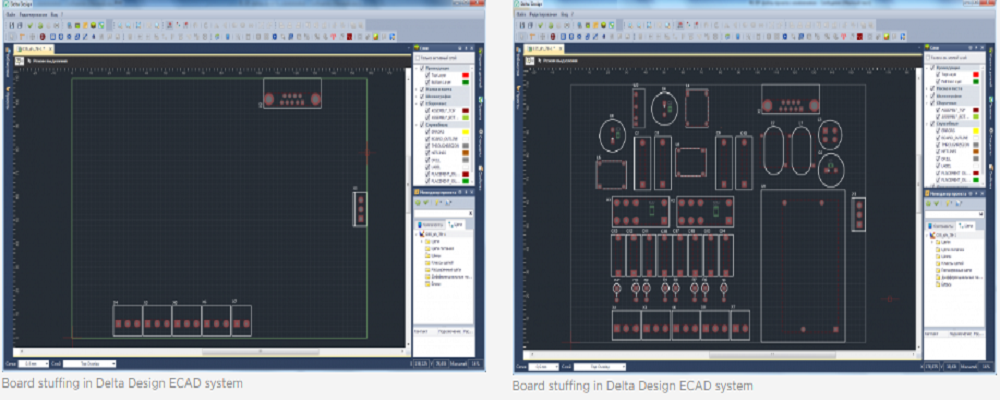
In the process of arranging the components and designing the topology (wiring), it is often necessary to carry out several iterative steps in which the board with the components is transferred to the 3D assembly of COMPAS-3D and back to the ECAD system. These procedures are performed by means of the ECAD-COMPAS Converter through the IDF format.
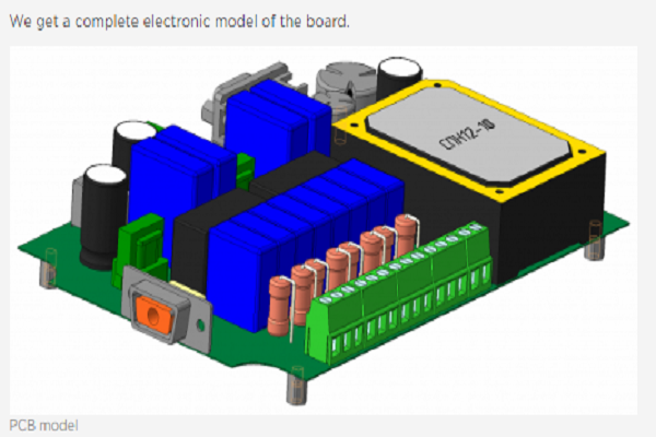
So, the dimensions of the board, the placement of components suits everyone, the trace is also completed. We turn back to KOMPAS-3D and finish working with the model of the printed circuit board. At this stage, the device designer not only re-receives the 3D model of the board, but also finalizes it in a certain way.
- Firstly, it is necessary to add information from the attributes of electronic radio products (ERI), which are stored in the ERI Database of the ECAD system, into the properties of the components of the board assembly. For this, the ECAD - KOMPAS Converter is also used. It receives information from text export files of the ECAD system and fills the properties of assembly components.
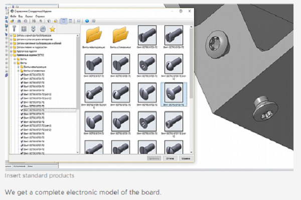
- Secondly, the board may include not only electronic components, but also mechanical components - racks, petals, brackets, radiators, etc. The device designer adds these products to the 3D-model of the board from local disks, from the LOTSMAN: PLM database, from the Standard Products Directory.
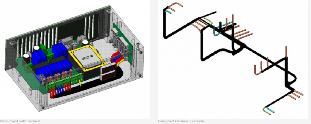
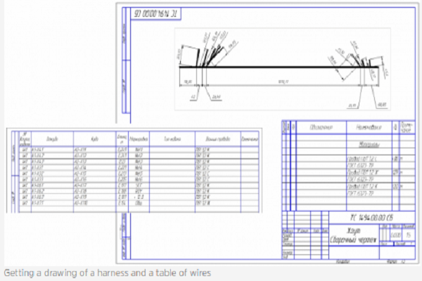
The designer of cable-harness strapping traces the wire harnesses and electric cables inside the product using the KOMPAS application Equipment: Cables and harnesses. Cable products are selected from the Materials and Assortments Directory. Connection tables and wire parameters can be obtained from the ECAD system or entered manually.
WE GET THE FULL ELECTRONIC STRUCTURE IN THE LOTSMAN: PLM
The device designer receives a 3D model of the product and its complete electronic composition in the PILOT: PLM.
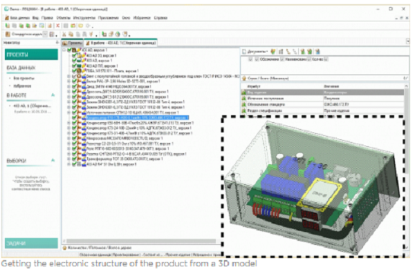
The structure contains Pilot objects with a set of files and various attributes that can be used in the future for a variety of tasks - to make selections according to certain criteria, to prepare reports.
WE CARRY OUT STRENGTH AND THERMAL CALCULATIONS
At the end of the purely design work on the product, calculations are required - strength, thermal, etc.
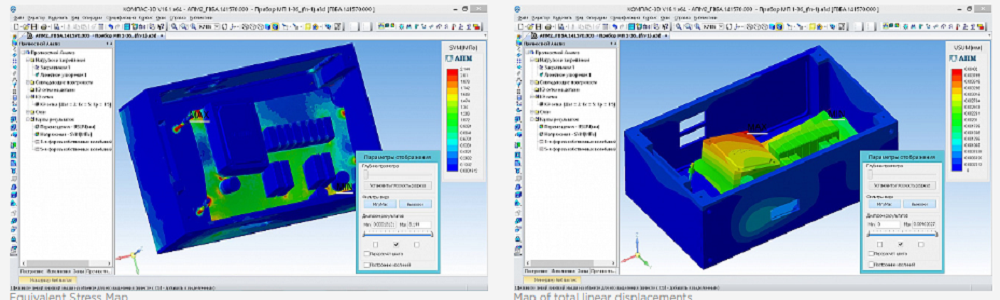
Strength calculations can be implemented in the APM FEM module, which is connected to KOMPAS-3D as a standard application. The calculator opens the model of the board in the application and performs a number of preparatory actions - defines the rules for the behavior of component models at one or another load, sets the location for fixing the model, and adds the actual load. This can be vibration loading with a certain frequency and acceleration, linear loads, torsional moments. Then a finite element grid is created, a calculation is made and models are formed with the results displayed on them, for example, the Map of equivalent stresses and the Map of total linear displacements.
Upon completion of all calculation procedures, their results can be stored in a single PILOT database: PLM. When specialists from different departments work as one team, in one database, they can always quickly see the results of their colleagues' work and take measures to rectify the situation in the event of unsatisfactory results.
WE RELEASE A FULL SET OF DESIGN DOCUMENTATION
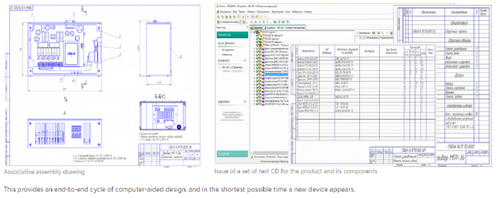
When the design and calculations are completed, and in LOTSMAN: PLM there is a complete set of objects, the designer creates a complete set of associative assembly drawings and detail drawings, and also automatically generates a set of textual design documentation for the product, including List of elements, BOM and List of purchased products. These documents are generated as KOMPAS files or as special report forms in the LOTSMAN: PLM. Moreover, the synchronization of documents with electronic structure allows you to automatically adjust them when changing the structure. Automation of these changes is allowed only until the design is completed. When a product enters the Archive stage, any changes to it are allowed only using the mechanism for issuing Change Notices
THE SOLUTION IS IMPLEMENTED ON THE BASIS OF PRODUCTS